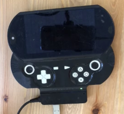
A few months ago, a contact reached out to me with an irresistible offer. I would be given the opportunity to experiment with an insanely rare, prototype development kit PlayStation Vita. The only ask from my source is that I somehow dump the boot code. I’ve spent the last seven years hacking every last bit of the Vita from exploiting the kernel to extracting hardware keys with AES fault injections. In that long journey, I’ve gotten intimate with every model and revision of the Vita so it seems inevitable that I would find myself with the very first prototype. The DEM-3000L is actually more rare than the DEM-3000H that recently made headlines having been sold for $20,000. Although I cannot confirm this independently, my source claims that the DEM-3000H units were distributed to early game developers while the DEM-3000L was used internally at Sony to develop the system firmware. The history of this particular DEM-3000L was that two of these were originally found side by side at a Chinese landfill. They had extensive water damage (I was told they were “at the bottom of a lake”) and was carefully repaired. One of the two (the one with the broken display) eventually made it to me.
I’ve been asked countless times: why dump the boot code? Especially on such a one-of-a-kind system? My first answer is that it’s because dumping the boot code is difficult and I never turn down an opportunity to flex on Twitter by posting cryptic hashes. My other answer is that in terms of preservation, there is historical value in attempting to extract as much data as possible out of this system before it deteriorates any farther. The Vita is a unique piece of hardware because everything is custom designed–from the hardware to the operating system to the executable formats. We’ve been obsessively documenting every tiny detail of this handheld console that was never the commercial hit that Sony wanted and anything that even adds a small drop of additional knowledge is worth it for me.
Previously on Vita glitching…
If you followed the Vita hacking scene, you might remember my foyer into hardware hacking by voltage glitching. I even wrote a paper documenting the whole procedure in academic (read: boring) detail. For the majority of you, here is a summary of what was needed to dump the boot code from a retail Vita. Recall that a glitch attack is simply a way to abuse transistor responses to extreme changes in the operating environment in order to cause the hardware to make “mistakes” in computation such as skipping or corrupting instructions being executed.
First serving
Initially, we had minimal knowledge about how the bootrom worked. We knew that it somehow loaded the bootloader (in a format called SLSK) from the eMMC, then parsed the bootloader header, checked the integrity/signatures, and finally jumped to the bootloader (after making sure bootrom code is no longer accessible). Every other documented software glitch attack either assumes that the attacker already has complete access to the code being executed or full understanding of how data is processed and can therefore device highly targeted glitches to bypass a certain check. For us, the story is more complicated. We cannot target a glitch on the signature check, for example, because we do not know when the signature check happens. Due to a bug in how Sony implemented the eMMC driver, 99% of the time spent in boot is waiting for the eMMC operation to complete, which makes the search space practically infeasible for blindly glitching and hoping to hit the right point. We did not have the public key to decrypt the signature nor did we have the encryption keys to decrypt the header (plus we did not even know where the signature resided in the file as it was mostly encrypted data).
To recast this problem in a more generic setting, we have to overcome two challenges in order to make use of a glitch attack to exploit software.
- We need an observable metric for success. How do you know if your glitch succeeded in changing the program behaviour? If you’re targeting a signature check bypass then it’s easy enough: wait for your code to be executed. But what if it fails? We can only pick glitch targets where success of the glitch can be measured independently from the success of the overall attack. If you have one condition for success and a dozen conditions for failure, then after days of glitching with different offsets and widths you end up learning nothing about the feasibility of your attack because any failure can be due to any reason.
- We need to be able to narrow down the search space for glitch parameters. The two parameters that makes the most impact in a crowbar voltage glitch are the offset (when the glitch is triggered) and the width (how long is the glitch). If the search space is too large, the turnaround time for experimentation would be days. In theory that is not too bad but in practice you’ll quickly lose morale when you see that multiple days passed and you have no idea if you’re even getting close.
The insight that we came up with eventually was that there appears to be a max size of the SLSK that is allowed. If the size is too large, the boot code refuses to load anything and panics. That size check was a great target because if we monitor the eMMC traffic, we can observe success by seeing the bootloader being read even though the size was too large. Since we know that the size check can only happen after the eMMC block containing the size field is read, we can set the glitch to trigger at some time offset after we observe that block being read. Additionally, if there is a size check, that usually means there is a buffer with a maximum size and if we bypass the check, we can overflow this buffer.
This plan worked and we discovered the buffer that we managed to overflow is actually adjacent to the code currently being executed so achieving code execution quickly followed.
But that was the end of the good news. We also discovered that there is no boot “rom” in the traditional sense. Instead what happens is that upon reset, some unknown hardware agent pre-loads the beginning of the SRAM with the boot code. Then the boot code copies itself to the end of the SRAM and jumps to it. At that point, the start of the SRAM becomes scratch space for the SLSK loading and that is why overflowing the buffer allows us to overwrite the currently running code. There is no evidence that the source for the initial boot code is ever mapped in memory so there’s no hope of getting it through software. Because our means of code execution requires overwriting this boot”ram”, we overwrite a lot of the code we are interested in. Even worse, the code was designed to wipe any secret from the SRAM as soon as it is used so we cannot dump those either even though they are not overwritten.
Second serving
Not all hope is lost though as we quickly discovered a second target after reverse engineering the code we got. As now documented on the wiki, Sony decided to re-use the start of the SRAM as a scratch buffer for loading the SLSK. Previously we overflowed this buffer in order to overwrite the adjacent code. Now we notice that the MeP processor has the exception vectors set to this same SRAM location and there is no way to turn off exceptions. Normally, Sony is safe because the only ways to trigger an exception aside from hardware signals are special instructions (software interrupts, debug breakpoints, etc) and divide by zero. The two times division is done in boot code is with a constant non-zero divisor and the special instructions are not found at all.
But with a glitch attack, it is easy to corrupt an instruction to hit one of these exceptions (the reserved instruction can be triggered especially easily with a glitch). In our second attack, we replace the first block of the SLSK bootloader with an exception vector that jumps into our payload. We trigger a glitch after the block is loaded and cause an exception. This works surprisingly well and much better than our original size-field attack because it doesn’t depend on a precise glitch on a single instruction. Instead, we can spray-and-pray random glitches with knowledge that any random instruction corruption will likely trigger the reserved instruction exception.
Most of the boot code was dumped this way, but since the block size of eMMC is 512 bytes, we still have to overwrite the first 512 bytes which destroys most of the initial startup code. Can we do even better?
Third serving
Turns out there is a very esoteric feature in Vita’s secure boot that we still do not fully understand the purpose of. second_loader.enp is the SLSK which is responsible for starting the ARM (main application) cores. Once ARM boots up, it locates and reads secure_kernel.enp from the eMMC and then does a handshake with F00D (the boot processor) to reset the core, which re-copies and re-starts the boot code. After reset F00D boot code loads secure_kernel.enp from the memory instead of second_loader.enp directly from the eMMC. secure_kernel.enp provides cryptographic services to the ARM processor.
Although this roundabout boot process is mysterious, we do not need to understand why it exists in order to exploit it. Recall in this alternative boot code path, the SLSK is copied directly from memory instead of read from eMMC (in 512 byte blocks). It copies 64 bytes of the SLSK file, verifies the header, and loads the rest of the file if the header check passes. If the check fails, it does not wipe the data so in effect we are still able to overwrite the exception vectors. This yields the following complicated procedure to get the remaining 448 bytes:
- Boot the Vita up normally using the HENkaku Ensō CFW to get kernel code execution.
- Privilege escalate to ARM TrustZone using a separate exploit.
- Pwn F00D with a third exploit in order to perform the reset handshake with TrustZone. This handshake requires both F00D code execution and ARM TrustZone code execution to pull off.
- Load the exception vector payload in TrustZone and trigger the glitcher with a sequence of characters written to UART console.
- After some time offset, the glitch happens and causes an exception in F00D which runs the payload.
So with 3 software vulnerabilities and a hardware glitcher, we can finally get 16320/16384 bytes of the boot code. The remaining 64 bytes? Turns out it is just the (original) exception table which is the same entry (to a panic) repeated 15 times. We also guess the reset vector (0x0) points to the only boot code in the system 😀.
Prototype glitching
Previously I bought a box of Vita motherboards to experiment on. I was able to make PCB modifications and do wild things that quickly killed the boards (such as accidentally shorting CORE_VDD to any other voltage source). With this rare prototype unit, we have to be more careful and so we cannot reproduce the exact same setup. For one, the retail Vita had the main SoC and the eMMC side by side so the wires between the two are relatively long and so Sony had to route in a couple of resistors for signal integrity. The way we probed the eMMC (both for recovering from bad payload flashes as well as for triggering the glitches) required soldering wires to these tiny resistors. On the DEM, the eMMC lies directly underneath the SoC on the opposite side of the board with the wires going through the board instead of across, making the signals impossible to probe. Secondly, there is a widely held belief that removing decoupling capacitors on the board will improve glitch success. At this point, I have not seen any convincing evidence that removing decoupling capacitors actually makes a difference for crowbar voltage glitching and it feels like cargo-culting to me. Therefore I make no attempt to find and remove decoupling capacitors. Finally, to replace the eMMC packet trigger, I decided to re-purpose an on-board debug LED because it was easy to control via software and because it seems least likely to make an impact if it was accidentally destroyed.
Narrowing the parameter search
As mentioned above, one of the two main challenges is to figure out when to trigger the glitch. We can toggle the LED as a trigger before the reset handshake but the SLSK load process takes anywhere from 10ms-22ms. Even worse, when the load fails for any reason, it will sleep for a random amount of time between 0ms and 4ms. 22ms does not seem like much but assuming each step width is 27ns (chosen because the external clock is 37MHz), we have 814,000 possible offsets times however many number of glitch widths we want to try. On the DEM because of all the debug logging, each boot takes around 45 seconds, so brute force checking is impracticable (more than a year to try all possible offsets for a single width).
We make the reasonable assumption that future predicts past and that the DEM boot code is similar to the retail boot code. Using xyz’s Ghidra plugin we can take a look at the disassembly of the DRAM SLSK load path.
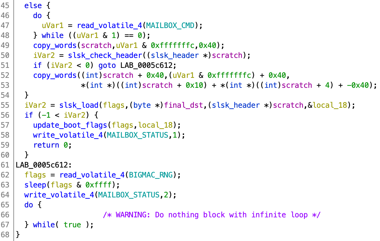
The SLSK address is read from ARM (and is saved in uVar1). It first copies in the 64 bytes header and checks it. If the check passes, it copies in the remaining SLSK file with the size computed from the header. We want to find the precise time when the header check happens because we place the payload into the SLSK header. To do this, we look into the disassembly for copy_words (the disassembly is better than the decompilation because timing matters here).
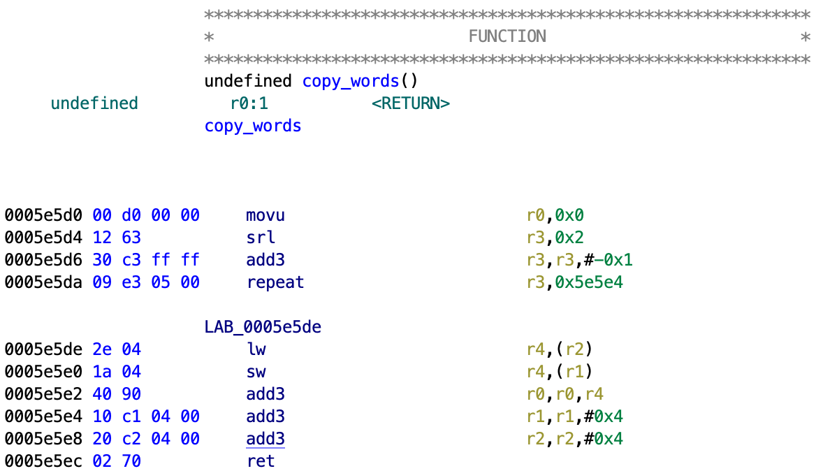
For those unfamiliar with MeP assembly, the repeat instruction will repeat all instructions until the address in the second operand plus an additional two instructions (delay slots) for the number of times specified in the register of the first operand. Basically this code loops and copies 4 bytes at a time from the user specified memory to the SRAM.
Because we know 4 bytes are read at a time, we come up with the following experiment: on the ARM side, we take a valid SLSK and corrupt the word at offset x. Then we trigger the reboot handshake and wait y cycles. After the wait, we “recover” the original word at offset x. If we wait too long, then the copy_word operation will read in the corrupted word at x and then fail to load the SLSK and we see return code 2. If we don’t wait long enough, then copy_word will read in the original word and because the SLSK is valid, we see a return code of 1. Now for each offset x, we vary the cycle count y until we find the lowest y that still returns status 2. This gives us an upper bound for the number of cycles to wait before the word at offset x is copied in. Then we do this for every x.
Now we do a second experiment which is a slight modification. We start with a valid SLSK, trigger the reboot handshake, and wait v cycles. After the wait, we corrupt the word at offset u. This time, if we wait too long, then copy_word will not see the corrupted word and return success status 1. If we don’t wait long enough, copy_word will see the corrupted word and return error status 2. This gives us a lower bound for the cycle offset from the reset handshake to when the word at offset u is copied in. We do this for every u.
Here is the plot for the first 500 bytes:
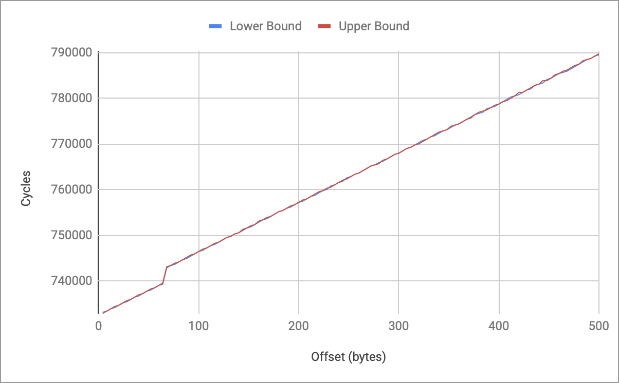
The first thing we see is that the lower bound and upper bound track each other well. This is important as it shows that our measurement has very small variance and gives us confidence in the results. Secondly, we see that the relationship is mostly linear with a small jump at 64 bytes. This matches the expected behaviour from the retail boot code: 64 bytes are read in first, the header is checked, then the remaining bytes are copied in (if the check passes). Finally, we see that the “jump” happens from 0xB4800 to 0xB5600 which becomes our window of interest if we expect to glitch past the header size field check. After translating cycle count to real time, we reduce the search space from 814,000 possible offsets to 400 possible offsets.
Observing success
The second challenge is to measure success. We have to do it without resorting to probing the eMMC. A key discovery was when we realized that any bus error (even those caused by the boot processor) will cause an interrupt to the ARM cores which (only on the DEM units) causes an error message to be printed out. Since the boot code does not do any address checks, if we put a valid SLSK at the edge of memory, then it will trigger a bus error message to be printed out when the read hits the end.
In order words, say we craft a valid SLSK header which specifies the size is 0x2000 and we put this header at 0x1F85F000. That region of memory ends at 0x1F85FFFF so when the boot code attempts to read in 0x2000 bytes, then after 0x1000 bytes it will go out of bounds and trigger a bus error message to be printed out.
How do we use this to measure if a glitch succeeded? We found through trial and error that the maximum size specified in the SLSK header is 0x1C000 bytes. Anything beyond that fails the header checks. So if we set the size to 0x1D000 and put the header at 0x1F844000, then when the glitch fails, the “remaining” data will not be read in and nothing happens. If the glitch succeeds, then the boot code will attempt to read 0x1D000 bytes but after 0x1C000 bytes it will hit the end of the memory region and we will see the bus error get printed out.
Since we wish to trigger an exception as soon as the SLSK header is read in and we know that the header size field is checked soon after, any time we successfully glitch the size field check also gives us information about when we can trigger the exception glitch. In effect, we use one glitch to gain information for future glitches.
Injected payload
In the final act, we create the payload the dumps the boot code. Through experimentation, we discovered that once the code reaches the while (1) dead-loop upon failure, the chances of an exception glitch is pretty much nil. (The technical explanation has to do with timing of critical paths and how shorter paths are less susceptible to fault behaviour.) In order to maximize the time between the header read and the dead-loop, we created an exception vector payload that passes the SLSK header check so it can reach the next phase of reading in the “rest of the SLSK”. We then try to cause an exception glitch while this is happening.
The way we do this is actually pretty simple. We took an existing SLSK header and tried to “disassemble” it as MeP code. We noticed that if we interpret the valid header as “code”, the instructions from offset 0x8 (where the reserved instruction exception vector resides) to offset 0x20 are benign and are essentially no-ops. The header check function does not check the data from offset 0x20 to 0x40 (in the real SLSK header, this contains a SHA-256 hash of the decrypted code) and we can use this space for our payload. 32 bytes is enough to jump to some region of memory we control where we copy out the boot code.

Pictured (top to bottom, clockwise): front shell of DEM disassembled, oscilloscope probes to see the glitches, ChipWhisperer Lite glitcher, breadboard hosting a single pullup resistor for LED GPIO trigger (ignore the unused/unrelated chip), Morgana, DEM unit under attack.
Putting this all together:
- Just as before, we use a ARM kernel exploit, ARM TrustZone exploit, and F00D exploit to gain execution in all three contexts.
- Our exception vector payload and the final boot code dumper code are placed in memory.
- We arm the hardware glitcher by a UART message. The next GPIO toggle will trigger the glitch. Arming the glitcher prevents accidentally glitching at the wrong time (i.e. when boot-up takes over the LED lights for example).
- The F00D reset sequence is triggered from ARM TrustZone and F00D. We pass in the address to our exception vector payload (masquerading as a SLSK header).
- We spin for exactly
0xB4800cycles (as determined by “narrowing the parameter search”). - The LED GPIO pin is toggled, this signals the hardware glitcher to trigger a glitch after some offset.
- We wait up to 10 seconds for the dump to appear over UART. If not, we choose a different set of glitch parameters (chosen amongst the results from “observing success”), restart the DEM and start over.
Offsets 240-250 with width 59 at glitch clock 37MHz can consistently trigger the payload. Note that these parameters are highly specific to our specific setup.
Resources
If you want to learn more about hardware glitching, the ChipWhisperer Wiki is a great place to start. If you get a ChipWhisperer Lite hardware, you can follow the tutorials there to learn more. Our work was all done on a ChipWhisperer Lite along with some molecule mods that enables features such as eMMC packet triggering, multiple glitch units, edge triggering with extra GPIO inputs, extra clock divider options, and more. You can also find some Vita-specific scripts for the ChipWhisperer for glitching and for DFA. Finally, if you want to learn more about the Vita, the HENkaku wiki is the place to go.
The DEM prototype glitching summarized in this article was done live on Twitch over exactly two weeks. If you want to see the whole process from inception to completion, they are all recorded in vods. Be warned though, more time was wasted going down wrong paths and making mistakes than actual progress–but that is how real hacking works. Thanks to everyone who tuned in and provided help and moral support, and to xyz for providing the exploit to trigger the reset handshake.
Congrats! Are you going to post a video of an actual successful glitch? I think those of us who watched the other unsuccessful videos would love to see it.
I thought about it but it looks no different from the countless times the test payload was executed.